The nanosphere lithography (NSL) method creates ordered arrays of nanostructures on a substrate using self-assembled monolayers of nanospheres as a mask. Here spin coating technique for nanosphere lithography for resulting patterned substrate can be used for a wide range of applications. Like increasing the sensitivity of Raman spectroscopy, where surface-enhanced Raman spectroscopy (SERS) uses ordered arrays of nanostructures with high surface area as substrates. In plasmonics, using NSL, plasmonic structures with clearly defined sizes and geometries may be made. These structures can then be employed in photovoltaic and biosensing systems, among other things. In the manufacture of nanoelectronic components including transistors, sensors, and memory devices can be done using patterns of nanoscale dimensions made using NSL on a substrate. For antireflection coatings, by forming nanoscale structures on a material’s surface, NSL can lessen reflection and boost light absorption. Applications like displays and solar cells may benefit from this. In biomaterials, NSL can be used to organise nanostructures into arrays on a material’s surface, enhancing its biocompatibility and encouraging cell adherence. Applications like tissue engineering and medicine delivery may benefit from this. NSL has the potential to be used in a variety of industries because it is a flexible and affordable method for creating nanostructures with excellent resolution and uniformity.
Procedure for Polystyrene Self assembled Monolayer by Spin coating Technique using the NT12000V1 for Nanosphere Lithography
- Monodispersed polystyrene (PS) colloids of diameter ~ 460 nm (10 wt% in water) were purchased from Sigma Aldrich.
- The PS suspension was further diluted to 2 wt% in methanol, and 0.025 wt% sodium dodecyl sulfate (SDS) (purest grade purchased from Merck, India) was added to the solution to stabilize the colloidal dispersion.
- Subsequently, 100 µl of the stabilized colloidal dispersion was dispensed drop by drop using a micropipette on the rotating Silicon substrate (1.2 cm * 1.2 cm) substrate at the spin speed of 600 RPM for 160 sec to remove the solvent altogether.
Progress of Honeycomb IBnC at CeNSE, IISC
Self-assembled colloidal nanospheres of ~ 450 nm diameter on Silicone substrate. Experiment performed by Dr. Adithya Sadhanala’s research team at CeNSE.
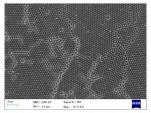
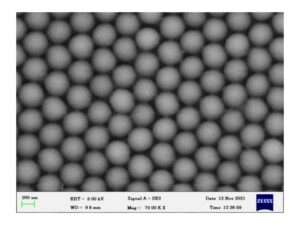
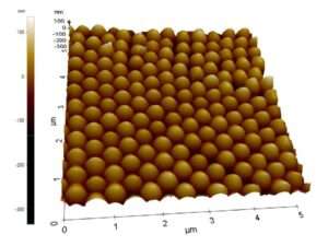
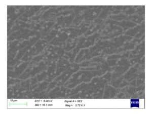
Layers formed on substrate by Spin Coating using NT12000V1
The creation of ordered arrays of PS spheres with controlled size and spacing using this method can be employed for a range of tasks, such as surface modification and nanoscale patterning.
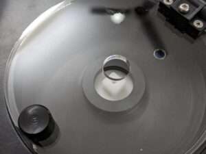
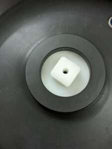
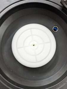
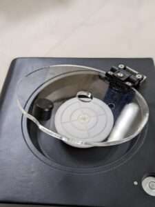
Navson Spin Coater Images
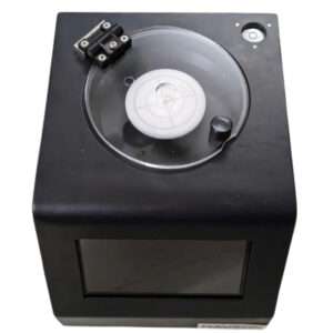
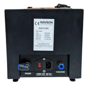
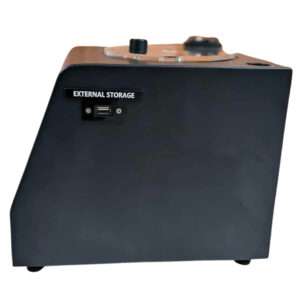
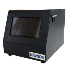
Spin coating Technique for Nanosphere Lithography
The spin coating process is an essential step in the production of a self-assembled monolayer (SAM) of polystyrene (PS) nanospheres for use as a mask in nanosphere lithography. It is a typical technique for applying thin material coatings to substrates because the dispersion forms a monolayer of tightly packed PS nanospheres due to the centrifugal force created by the rotation of the substrates during the spin-coating process.
